


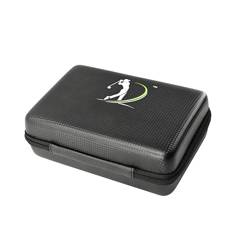
Custom-designed EVA kits for precision chip testing instruments
In today’s rapidly evolving semiconductor industry, precision chip testing instruments are core equipment in chip R&D, production, and quality inspection. Their accuracy and stability directly determine the yield and performance of chip products. These instruments integrate high-precision sensors, miniature optical components, and sensitive circuit modules, making them extremely sensitive to external interference such as vibration, static electricity, moisture, and impacts during transportation, storage, and field operations.
Traditional general-purpose packaging often fails to meet their stringent protection requirements. Customized EVA kits, with their precise adaptability, multi-functional protection capabilities, and compliant design, are becoming the preferred solution for global semiconductor companies to protect their precision testing instruments.
I. Protection Challenges for Precision Chip Testing Instruments: Why General Packaging Falls Short The application scenarios for precision chip testing instruments span multiple stages, including laboratory R&D, production line quality inspection, and cross-border delivery. The protection requirements in different scenarios are highly complex:
Threats of High-Frequency Vibration and Shock:During long-distance transportation or on-site movement, vehicle bumps and manual handling can easily cause optical lens misalignment, sensor calibration parameter failure, and even circuit solder joint detachment. Traditional foam packaging lacks sufficient cushioning performance and cannot absorb high-frequency, multi-angle external impacts.
Hidden Risks of Electrostatic Discharge:The core components of chip testing instruments are extremely sensitive to static electricity. Even a small release of static electricity can break down precision circuits, causing irreversible damage. Ordinary packaging materials lack anti-static properties; static electricity generated in dry environments or during friction can become a “hidden killer” for the instruments.
Corrosive Effects of Temperature and Humidity Changes:Whether it’s the high-humidity salt spray environment during sea transport or the extreme temperature differences in deserts and frigid regions, internal components of the instruments can become damp and age, affecting testing accuracy. General packaging lacks targeted moisture-proof and temperature control designs, making it difficult to adapt to diverse application scenarios. The problem of insufficient component compatibility: Chip testing instruments often come with various accessories, such as testing probes, calibration fixtures, and data cables. The cluttered storage design of generic packaging easily leads to lost accessories or damage from collisions with the main unit, affecting work efficiency.
II. Customized EVA Toolkit: Three Core Advantages Create a Dedicated Protective Armor
Addressing the protection pain points of precision chip testing instruments, the customized EVA toolkit constructs a comprehensive protection system from three dimensions: materials, processes, and functions, achieving the dual value of “precise protection + efficient compatibility.”
1. Material Upgrade: A Leap from Basic Protection to Functional Protection
EVA (ethylene-vinyl acetate copolymer) material itself possesses lightweight, high elasticity, and wear-resistant properties. For the customized needs of precision chip testing instruments, material modification and process optimization can further endow the tool bag with more professional protective functions:
Superior Cushioning and Shock Absorption: The customized EVA foam adopts a closed-cell structure design, increasing the resilience coefficient by 40% compared to traditional EPE foam. It can absorb over 90% of high-frequency impacts during transportation and withstand drops from a height of 1.2 meters without damaging internal instruments. Even during complex cross-border logistics transit, it effectively isolates external interference.
Special Anti-static Protection:Utilizing conductive carbon black modification technology, the surface resistance of the customized anti-static EVA foam can be stably controlled at 10^6 – 10^9 Ω, fully meeting the ESD protection standards for chip testing instruments and eliminating the risk of electrostatic breakdown at its source. Simultaneously, an anti-static flocking layer can be added to the inner wall of the tool bag to further enhance the protection level and tactile feel.
Stable performance in terms of moisture and weather resistance: EVA material itself has excellent waterproof and moisture-proof properties. Combined with sealed zippers and waterproof sealing technology, it can achieve IPX4 level waterproof protection. Even in marine environments with humidity up to 80% or in outdoor working environments during the rainy season, it can keep the internal instruments dry.
Globally compatible and environmentally compliant: Customized EVA toolkits strictly comply with EU PPWR packaging regulations, with a recyclability rate of no less than 65%. Through physical recycling technology, it reduces the carbon footprint by 60% compared to traditional foamed plastics. At the same time, the product has passed multiple international certifications such as CE, RoHS, and REACH, meeting market access standards around the world.
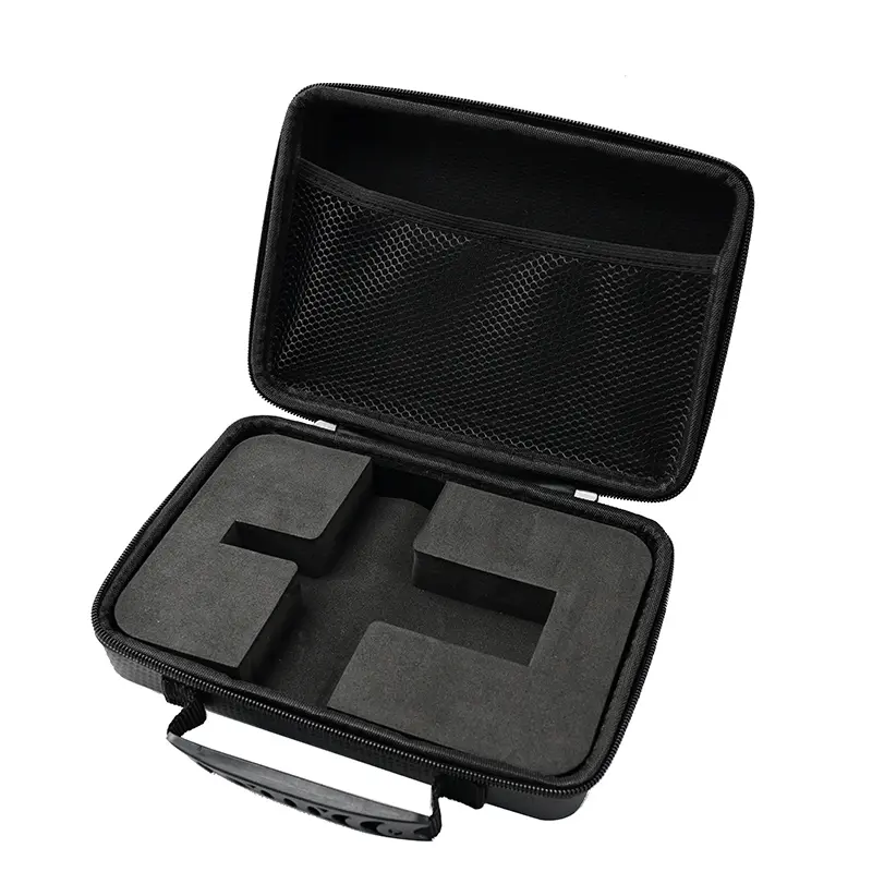
2. Customized process: Millimeter-level precise fit, achieving a seamless fit between “instrument and toolkit” The complex shape and structure of precision chip testing instruments, with unique distribution of components such as sensors, operation panels, and interfaces, make it difficult for general packaging’s “rough” protection to cover all vulnerable areas. Customized EVA toolkits utilize advanced processing technology to achieve millimeter-level replication of instrument contours:
High-precision die-cutting: Employing CNC engraving and laser cutting technology, processing accuracy reaches 0.1mm. Based on the instrument’s 3D modeling data, precise grooves are cut into the EVA foam, ensuring each component fits into its designated slot, completely eliminating shifting and shaking during transportation. Independent cushioning layers can be designed for vulnerable areas such as protruding lenses and interfaces, enhancing protection.
Layered and partitioned storage design: A multi-level, multi-partition spatial layout is adopted to accommodate the different sizes and functions of the instrument main unit and accessories. The main unit area ensures precise fit and fixation, while the accessory area features dedicated slots designed for probes, data cables, and calibration tools, preventing accessory loss and collisions with the main unit, improving on-site retrieval efficiency.
Personalized appearance and brand enhancement: Customization of the toolkit’s appearance color and surface texture is supported. Company logos and instrument model identifiers can be added through embossing, silkscreen printing, and other processes. This not only enhances product recognition but also conveys a professional brand image in scenarios such as customer acceptance and trade show presentations.
3. Functional Expansion: Adapting to Diverse Application Scenarios
Customized EVA toolkits can be equipped with diverse functional designs based on the actual application scenarios of chip testing instruments, meeting the usage needs of different scenarios such as laboratories, production lines, and cross-border transportation:
Portable Design: Utilizing lightweight EVA material and an ergonomic handle design, it balances protection and portability, making it convenient for technicians to carry instruments for on-site testing and customer on-site debugging.
High-Strength Shell Protection: The outer layer can be equipped with a hard ABS or PP material shell, enhancing the toolkit’s resistance to pressure and punctures, protecting the internal instruments from crushing damage even when stacked and transported in complex industrial environments.
Compliant Transportation Design: For cross-border transportation needs, the toolkit can be designed according to international sea and air freight packaging standards, equipped with a lithium battery storage compartment compliant with UN38.3 certification (if the instrument contains a lithium battery module), and marked with multilingual warning labels to ensure smooth customs clearance and avoid the risk of cargo seizure due to non-compliant packaging.
III. Full-Process Customization Service: A One-Stop Solution from Needs Communication to Delivery The customized protection requirements of precision chip testing instruments require a professional team and a comprehensive service system. Professional EVA toolkit customization service providers can provide full-process services from solution design to mass production delivery, ensuring the final product accurately matches customer needs:
Needs Research and Solution Design: A professional engineering team conducts in-depth communication regarding the instrument’s dimensions, protection pain points, application scenarios, and other requirements. Combining 3D modeling technology, they produce visual lining design schemes and appearance renderings, ensuring customers intuitively understand the product structure and protection effect.
Rapid Prototyping and Verification Adjustment: Support for small-batch sample production allows customers to conduct on-site testing using samples to verify key indicators such as lining fit, cushioning performance, and anti-static effect. For any issues discovered during testing, the engineering team responded quickly and made adjustments until the solution fully met the requirements.
High-efficiency mass production and rigorous quality control: With standardized production workshops and a mature supply chain system, we can achieve production with a minimum order quantity of 500 pieces and a mass production cycle controlled within 20 days. Each batch of products undergoes rigorous dimensional inspection, pressure resistance testing, anti-static testing, and other multiple quality control processes to ensure stable product quality.
Global logistics and after-sales support: Relying on a comprehensive international logistics cooperation system, we support product delivery worldwide. We also provide after-sales tracking services, offering timely technical support and solutions for any problems encountered by customers during use.
IV. Application Value: More than just protection, it optimizes efficiency and cost. The value of the EVA toolkit for precision chip testing instruments lies not only in the safety protection of the instruments but also in creating additional value for enterprises from multiple dimensions:
Reduced instrument wear and tear costs: Through precise protection, we significantly reduce the damage rate of instruments during transportation and storage, reduce the cost of repair and replacement parts, and extend the service life of the instruments.
Improve operational efficiency: The layered and zoned storage design makes it easier to access and store the main unit and accessories, reducing on-site preparation time and improving testing efficiency.
Strengthen brand professional image: Customized appearance design and brand logo can showcase the company’s professional capabilities in customer service, industry exhibitions, and other scenarios, enhancing brand recognition.
Post time: Jan-23-2026